Difference between revisions of "Debugging electronics"
(→MOSFET) |
|||
| Line 208: | Line 208: | ||
<br> | <br> | ||
The MOSFET has “gate“, “Drain” and “Source” terminals instead of a “base”, “collector”, and “emitter” terminals in a bipolar transistor. By applying voltage at the gate, it generates an electrical field to control the current flow through the channel between drain and source, and there is no current flow from the gate into the MOSFET. | The MOSFET has “gate“, “Drain” and “Source” terminals instead of a “base”, “collector”, and “emitter” terminals in a bipolar transistor. By applying voltage at the gate, it generates an electrical field to control the current flow through the channel between drain and source, and there is no current flow from the gate into the MOSFET. | ||
| + | <We will focus on N channel MOSFETS> | ||
<br> | <br> | ||
'''Depletion Mode''' – It requires the Gate-Source voltage ( Vgs ) applied to switch the device “OFF”. | '''Depletion Mode''' – It requires the Gate-Source voltage ( Vgs ) applied to switch the device “OFF”. | ||
Revision as of 07:56, 17 July 2019
Testing
As a test circuit we will build our own continuity tester, using the 555 timer IC
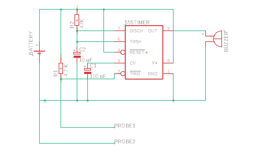
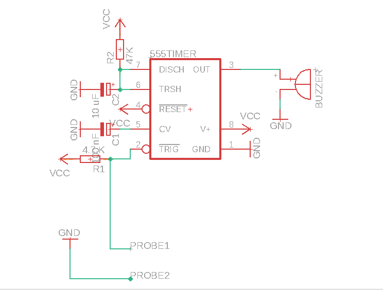
555 Timer operation in ASTABLE mode
The astable mode is what most people think of when it comes to the 555 timer. Many times when you see a project with flashing LEDs, it’s a 555 timer at work. But it has a lot of other interesting applications too. For example, it can also generate frequencies to produce sound when the output is connected to a speaker.
Pin 2 – Trigger: Turns on the output when the voltage supplied to it drops below 1/3 of Vcc
Pin 6 – Threshold: Turns off the output when the voltage supplied to it reaches above 2/3 Vcc.
Pin 7 – Discharge: When the output voltage is low, it discharges C1 to ground.
In astable mode, the output cycles on and off continuously. In the schematic above, notice that the threshold pin and the trigger pin are connected to C1. This makes the voltage the same at the trigger pin, threshold pin, and C1.
Case 1—if there is a break in circuit
If this case arises then that means there is infinite resistance (open circuit) between pin 2 and ground (no continuity between probes) which causes all voltage drop between pin 2 and ground which is obviously greater than 1/3 of 9 volt, so we get 0 volt as output from pin 3 at which buzzer Hence buzzer will produce no sound indicating a break in circuit.
Case2—if there is no break in circuit
If this case arises then that means there is almost 0 volts (short circuit) between pin 2 and ground (there is continuity between probes) which causes all voltage drop across 4.7k resistor and thus pin 2 gets 0 volts which is obviously less than 1/3 of 9 volt, so we get 1 volt as output from pin 3 at which buzzer is connected. Hence buzzer will produce sound indicating continuity in circuit.
Always check first
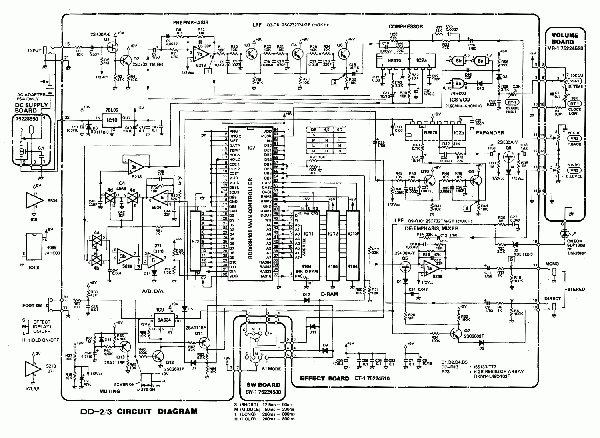
- do you understand the schematic (or image)
- power
- connections (soldered or breadboarded) If any dry soldering, solder bridges, any potential shorting or open PCB track issues are there?
- polarities. If any component is connect in reverse polarity, pin one of Microcontroller is soldered to pin one of the microcontroller PCB pad, etc.
- If all components are of desired value?
Understanding schematics
We will watch a short lynda video (which you can easily go back to with your student account) here
a good guide in reading chematics
Breadboarding and breadboard debugging
OK, first, what's with the name....bread board? Bread, like in food?
Well yes, kind of.

This terminology goes way back in the days.
Generally, you would mount electronic components to a piece of wood (the actual "breadboard"), and do all the wiring with point-point wire and the components just hanging between the various devices.
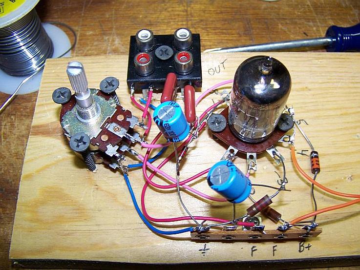
The story goes that an engineer had an idea for a vacuum tube device late one night. Looking around the house, the only base for his prototype that he found was indeed his wife's breadboard, from the breadbox.
A video by the Make magazine people
Ok, but why do we need to breadboard?
Well, they are useful for making temporary circuits and prototyping, and they require absolutely no soldering.
Prototyping is the process of testing out an idea by creating a preliminary model from which other forms are developed or copied, and it is one of the most common uses for breadboards.
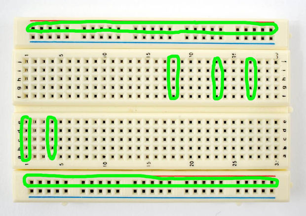
The best way to explain how a breadboard works is to take it apart and see what’s inside.
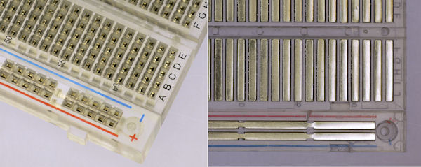
connections lines are connected like this
Tools for debugging
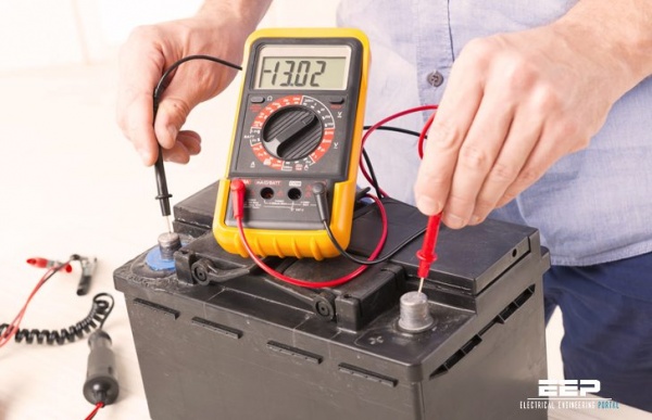
Multimeter
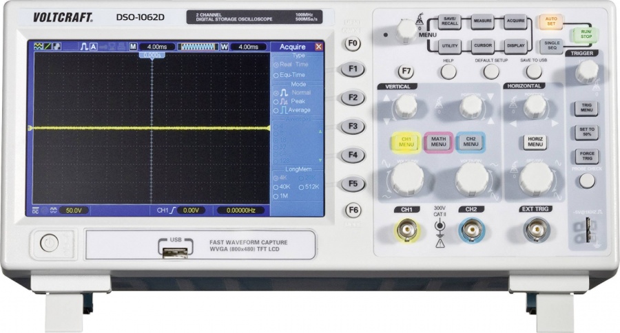
Oscilloscope
Transistors
BJT
the bi-polar junction transistor
In small, discrete quantities, transistors can be used to create simple electronic switches, digital logic, and signal amplifying circuits. In quantities of thousands, millions, and even billions, transistors are interconnected and embedded into tiny chips to create computer memories, microprocessors, and other complex ICs.
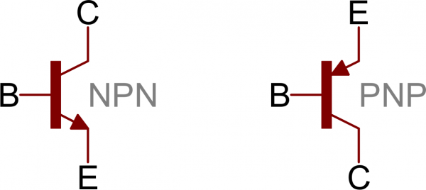
Transistors are fundamentally three-terminal devices. On a bi-polar junction transistor (BJT), those pins are labeled collector (C), base (B), and emitter (E). The circuit symbols for both the NPN and PNP BJT are:
as Switches
One of the most fundamental applications of a transistor is using it to control the flow of power to another part of the circuit -- using it as an electric switch. Driving it in either cutoff or saturation mode, the transistor can create the binary on/off effect of a switch.
Transistor switches are critical circuit-building blocks; they're used to make logic gates, which go on to create microcontrollers, microprocessors, and other integrated circuits.
The BC547 as a case study
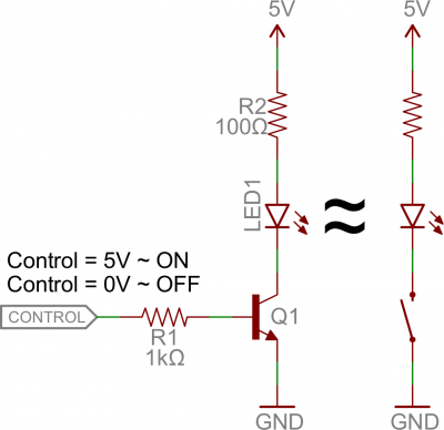
The control input flows into the base, the output is tied to the collector, and the emitter is kept at a fixed voltage.
While a normal switch would require an actuator to be physically flipped, this switch is controlled by the voltage at the base pin. A microcontroller I/O pin, like those on an Arduino, can be programmed to go high or low to turn the LED on or off.
When the voltage at the base is greater than 0.6V (or whatever your transistor's Vth might be), the transistor starts saturating and looks like a short circuit between collector and emitter. When the voltage at the base is less than 0.6V the transistor is in cutoff mode -- no current flows because it looks like an open circuit between C and E.
The circuit above is called a low-side switch, because the switch -- our transistor -- is on the low (ground) side of the circuit. Alternatively, we can use a PNP transistor to create a high-side switch:
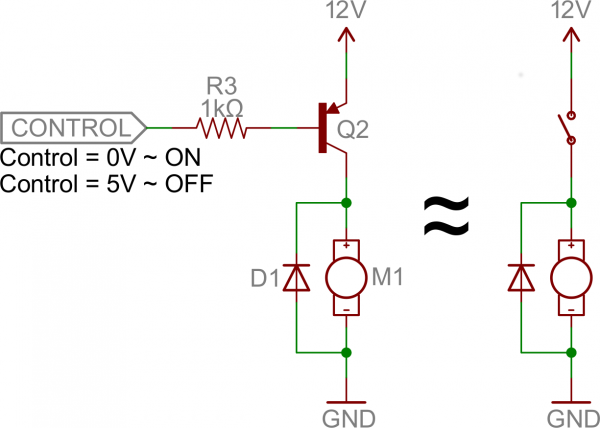
Similar to the NPN circuit, the base is our input, and the emitter is tied to a constant voltage. This time however, the emitter is tied high, and the load is connected to the transistor on the ground side.
This circuit works just as well as the NPN-based switch, but there's one huge difference: to turn the load "on", the base must be low. This can cause complications, especially if the load's high voltage (VCC being 12V connecting to the emitter VE in this picture) is higher than our control input's high voltage. For example, this circuit wouldn't work if you were trying to use a 5V-operating Arduino to switch off a 12V motor. In that case, it'd be impossible to turn the switch off because VB (connecting to the control pin) would always be less than VE .
Base Resistors
again Base Resistors!
You'll notice that each of those circuits uses a series resistor between the control input and the base of the transistor. Don't forget to add this resistor! A transistor without a resistor on the base is like an LED with no current-limiting resistor.
Recall that, in a way, a transistor is just a pair of interconnected diodes. We're forward-biasing the base-emitter diode to turn the load on. The diode only needs 0.6V to turn on, more voltage than that means more current. Some transistors may only be rated for a maximum of 10-100mA of current to flow through them. If you supply a current over the maximum rating, the transistor might blow up.
R=(V-Vbe)/Ib
To calculate the base resistor for an led controled by an Arduino we need to know the following:
The V is the 5V coming from the Arduino pin, the Vbe is the Saturation Voltage (from the datasheet) = 700 mA, the Ib is the base current. When transistor is used as a switch, it is common to assume that base current is 1/10 of the collector current.
If the collector current is 20mA, then base current should be 2mA.
So R= (5-0.7)/0.002
Which is 2.150 so a 2K resistor will be a good value
This is actually a fundamental transistor configuration called common emitter
As Amplifiers
Some of the most powerful transistor applications involve amplification: turning a low power signal into one of higher power. Amplifiers can increase the voltage of a signal, taking something from the µV range and converting it to a more useful mV or V level. Or they can amplify current, useful for turning the µA of current produced by a photodiode into a current of much higher magnitude.
Three of the most fundamental transistor amplifiers are: common emitter, common collector and common base. In each of the three configurations one of the three nodes is permanently tied to a common voltage (usually ground), and the other two nodes are either an input or output of the amplifier.
Common Configurations
Three of the most fundamental transistor amplifiers are: common emitter, common collector and common base(not included here:). In each of the three configurations one of the three nodes is permanently tied to a common voltage (usually ground), and the other two nodes are either an input or output of the amplifier.
Common Emitter
Common emitter is one of the more popular transistor arrangements. In this circuit the emitter is tied to a voltage common to both the base and collector (usually ground). The base becomes the signal input, and the collector becomes the output.

The common emitter circuit is popular because it's well-suited for voltage amplification, especially at low frequencies. They're great for amplifying audio signals, for example.
Common Collector (Emitter Follower)
If we tie the collector pin to a common voltage, use the base as an input, and the emitter as an output, we have a common collector. This configuration is also known as an emitter follower.

The common collector doesn't do any voltage amplification (in fact, the voltage out will be 0.6V lower than the voltage in). For that reason, this circuit is sometimes called a voltage follower.
This circuit does have great potential as a current amplifier. In addition to that, the high current gain combined with near unity voltage gain makes this circuit a great voltage buffer. A voltage buffer prevents a load circuit from undesirably interfering with the circuit driving it.
JFET
In the Bipolar Junction Transistor tutorials, we saw that the output Collector current of the transistor is proportional to input current flowing into the Base terminal of the device, thereby making the bipolar transistor a “CURRENT” operated device as a smaller current can be used to switch a larger load current.
The Field Effect Transistor, or simply FET however, uses the voltage that is applied to their input terminal, called the Gate to control the current flowing through them resulting in the output current being proportional to the input voltage. As their operation relies on an electric field (hence the name field effect) generated by the input Gate voltage, this then makes the Field Effect Transistor a “VOLTAGE” operated device.
SIMPLIFIED
A FET turns on "more" as gate to source voltage goes higher, there is virtually no current flowing into gate.
A BJT turns on "more" as base to emitter current goes higher, there is a virtually constant 0.6V across base and emitter.
FETs in general, source-drain current is controlled with a very little current from the gate.
BJTs require more current, because of how it works, collector-emitter current is proportional to the current from the base.
MOSFET
MOSFET stands for metal-oxide semiconductor field-effect transistor. It is a special type of field-effect transistor (FET).
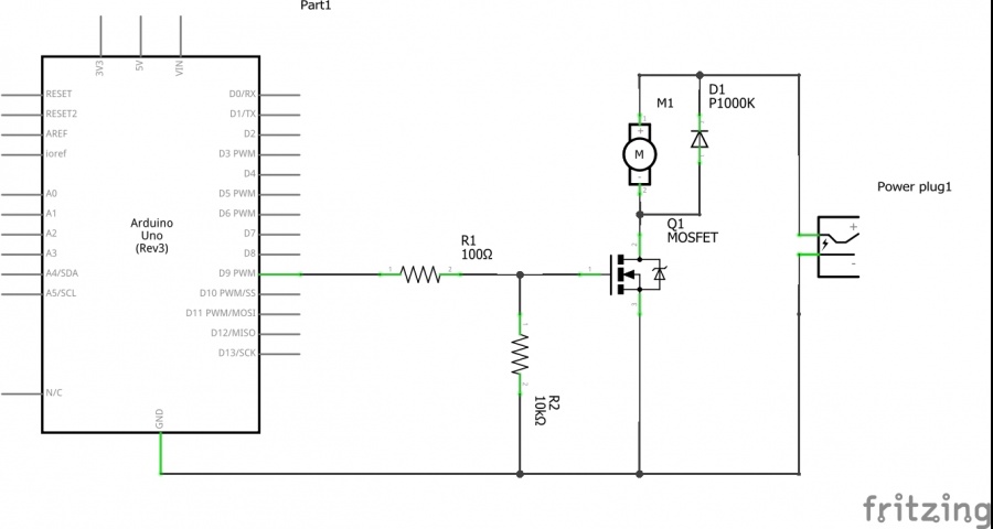
The MOSFET has “gate“, “Drain” and “Source” terminals instead of a “base”, “collector”, and “emitter” terminals in a bipolar transistor. By applying voltage at the gate, it generates an electrical field to control the current flow through the channel between drain and source, and there is no current flow from the gate into the MOSFET.
<We will focus on N channel MOSFETS>
Depletion Mode – It requires the Gate-Source voltage ( Vgs ) applied to switch the device “OFF”.
Enhancement Mode – The transistor requires a Gate-Source voltage ( Vgs ) applied to switch the device “ON”.
Despite the variety, the most commonly used type is N-channel enhancement mode.
Logic Level MOSFETS
Vth Treshold Voltage
When using a MOSFET, controlled by a microcontroller, we need to consider using a Logic level MOSFET. That means it will have a low Treshhold Voltage, menaing it will requite a relatively small Gate Voltage to start conducting.
Vth is something that is determined during the MOSFET fabrication process. However, due to practical conditions and fabrication imperfections, you will never get a perfect constant Vth for a MOSFET. Thus, there is always a range of Vth. Vth of 2-4 V means that the threshold voltage of your MOSFET will vary in 2-4 V range.
Id Drain Current is the maximum current it can pass in the forward direction.
Where to put the load to a MOSFET? Source or Drain?
Because the load has resistance, which is basically a resistor. For N-channel MOSFET the reason we usually put the load at the Drain side is because of the Source is usually connected to GND.
If the load is connected at the source side, the Vgs will needs to be higher in order to switch the MOSFET, or there will be insufficient current flow between source and drain than expected.

