Difference between revisions of "Board layout in Eagle"
| Line 29: | Line 29: | ||
==copper pours== | ==copper pours== | ||
| − | [[Category:Electronics]][[Category:Making]] | + | [[Category:Electronics]][[Category:Making]][[Category:Eagle]] |
Revision as of 09:10, 21 November 2022
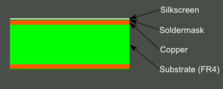
Layers
PCB composition is all about layering one material over another. The thickest, middle part of the board is a insulating substrate (usually FR4). On either side of that is a thin layer of copper, where our electric signals pass through. To insulate and protect the copper layers, we cover them with a thin layer of lacquer-like soldermask, which is what gives the PCB color (green, red, blue, etc.). Finally, to top it all off, we add a layer of ink-like silkscreen, which can add text and logos to the PCB.
Arranging the board
The Grid
In the schematic editor we never even looked at the grid, but in the board editor it becomes much more important. The grid should be visible in the board editor.
EAGLE forces your parts, traces, and other objects to "snap" to the grid defined in the Size box. If you need finer control, hold down ALT on your keyboard to access the alternate grid, which is defined in the Alt box.

