Etching
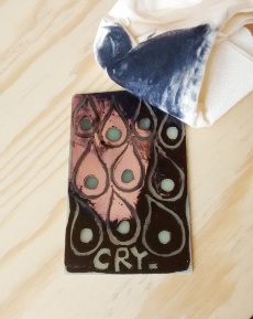
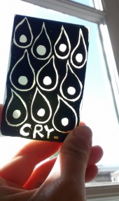
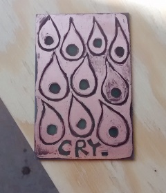
Etching is traditionally the process of using strong acid or mordant to cut into the unprotected parts of a metal surface to create a design in in the metal.
It is is a print making method. The reason you find it in our wiki, is that...electronics and the handmade craft of etching are tied up together.
Etching is also a method used in handmade circuit making.
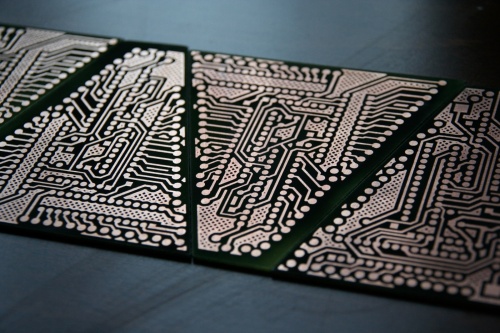
Etching is a "subtractive" method used for the production of printed circuit boards: acid is used to remove unwanted copper from a prefabricated laminate. This is done by applying a temporary mask that protects parts of the laminate from the acid and leaves the desired copper layer untouched.
It's easy and can be done in a home environment ( being careful, due to the use of poisonous chemicals).
There are different ways to make a mask on the material, meaning to cover the parts of the copper we want to use for our circuit.
Toner Transfer
The circuit layout is printed with a laser printer on paper, put face-down on the laminate, and the toner is transfered from the paper to the copper using an iron.
Not every paper is suited for this method, mostly promoted are magazine pages or other glossy papers.
The print must be of a very good quality. The transfer of the toner is a bit tricky. If temperature is too high, the toner gets too liquid and the tracks will blur. If the temperature is too low, the toner won't stick to the copper. After the ironing you can't pull the paper away just like that, without destroying half of the mask. Instead you have to put the laminate with the paper in a water bath and wait a while until you can start to scrub away the paper. This may take quite some time, so be patient.
Photo-resist coatings
A photo-sensitive layer covers the copper board. The mask (circuit design) is printed on a transparent paper or foil, exposed and developed on the laminate with a UV lamp.
The coating is sensitive to light. We either cover the board with it ourselves (you get it separately) or get a board that is already photo-sensitive. By shining a light on the board, covered with photo-resist, we can transfer an image of the design to be created onto the board. Depending on the coating it may be that where light strikes the board, the coating weakens and creates an area of copper that will be dissolved away by the etching acid. OR the other way around. So your design depends on how the coating reacts to light. NOTE the design may have to be inverted and has to be mirrored:)
The first step is to make a board layout. Misschien using Eagle (CAD software), although the learning curve can be a bit steep. The SparkFun tutorials seem good [1].
Then, one workflow would be to hide all layers in Eagle except the bottom traces, then print it to a PDF. Works good because it's very high pixel density. That's critical to getting small traces to work. In the beginning may be better to make the traces a bit thicker just in case .
Next, print on regular paper and check the scale and orientation of your design. Just in case, if you are overconfident, skip this:)
Then print with a laser printer onto a transparent sheet. The black needs to be very black! A good idea is to print it twice and very carefully stick them together, perfectly matching, so the layer of black will become thicker and will better prevent light from entering.
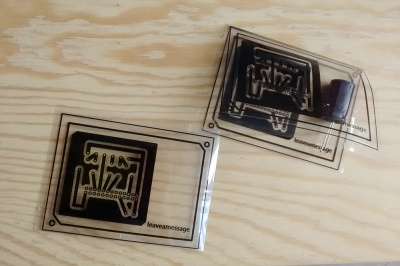
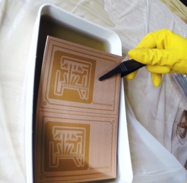
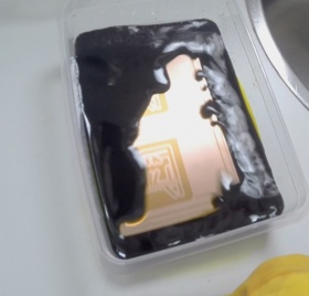
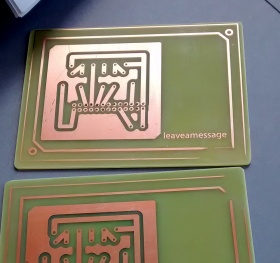
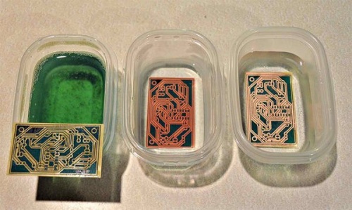
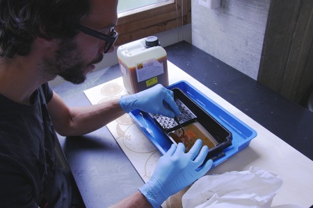
1. the etching mask printed on transparent inkjet sheet 2. after being exposed, it is developed and the solder mask shows up 3. etching away the uncovered copper in ferric chloride 4. ready, drilled boards
p.s. its a first etching test with very thick traces:)
Vinyl masking
This strategy so far proves to be very good.
Using a vinyl cutter to make an etch mask, produces nice results:)
We used a Silhouette Cameo vinyl cutter with a rather blunt knife.
PLUSESSSS:
- Is quite faster.
- No need to go into exposing and developing, so...using less chemistry and getting dirty less.
- You get clear and sharp edges, if the blade is in sharp.
MINUSESSS:
- Small, precise details may not be brilliant, depending on the cutter and mostly sharpness of the blade
- Lines cannot get too thin, unless you are a master craftsman.
- Double sided etching is trickier
it is important to stick the vinyl very well to the board, removing all air bubbles, otherwise chemical may enter and touch the surface and eat away the copper.
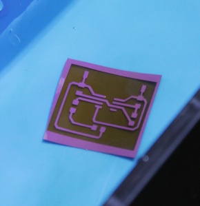
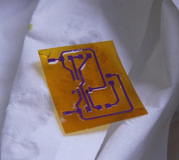
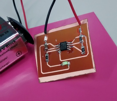
Simon making a test, that turned out very good. It is a smd 555 timer led blinker.
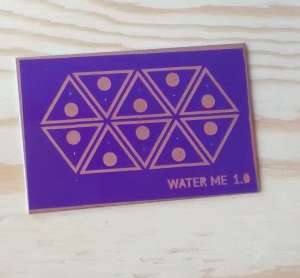
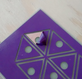
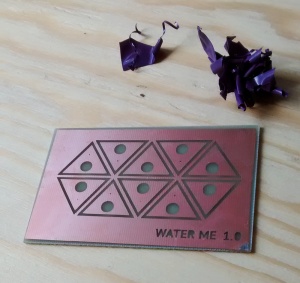
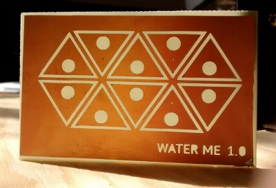
1. the mask on the copper. 2. after etching, peeling off the vinyl 4. aaand Voila .... A circuit for an open aanbod class
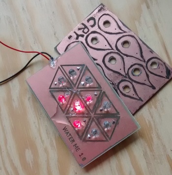
And the ready boards!
Sharpie resist technique
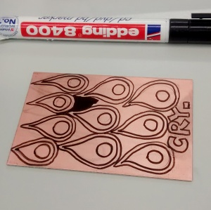
This method is rather straightforward. Using a permanent marker, to draw by hand the etch mask, a.k.a. hand drawn pcb!
Something that applies a thicker line of paint might survive the etchants better, according to online sources, a Sharpie proves to be good. We used an Edding marker.
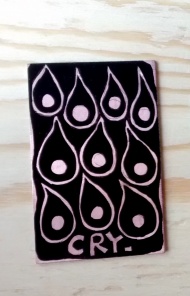
Produces slightly grungy results, but looks beautifully hand drawn and has a tactile feel.
1. drawn outlines 2. finished drawing 3. after etching clean the marker with some acetone or nail polish remover 4. and the copper is gone 5. cleaned
Laser engraved painT coating
In short, in this method, a copper pcb is spray painted and then the etching mask is engraved with a Laser cutter machine.
a first failed try!
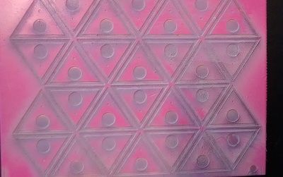
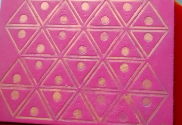
Mistakes:
- painted two layers of paint, thus there was more material to remove and the paint dust was more, then it was stuck on the board and cannot be removed
- tried removing the paint dust with acetone, so it damaged the actual mask.
- used a slow speed of engraving.
